
TL;DR
Researchers from Longi and Yangzhou University have developed a heterojunction back-contact solar cell with a certified efficiency of 27.27%. The breakthrough involves a new laser manufacturing method that reduces damage caused by shock waves, bringing ultra-high-efficiency photovoltaics closer to industrial production.
Researchers from Longi and Yangzhou University have developed a heterojunction back-contact solar cell with a certified efficiency of 27.27%, using a novel laser-based manufacturing process that reduces shock wave damage. This advancement demonstrates a practical pathway toward ultra-high-efficiency photovoltaic devices suitable for industrial application.
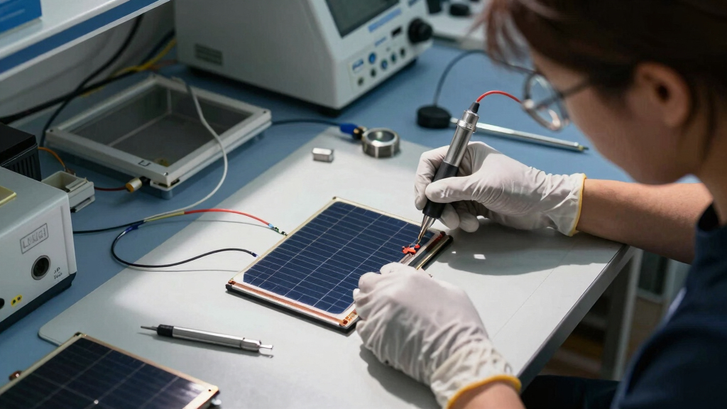
The team addressed a key challenge in laser processing—shock wave-induced damage—by identifying the role of the rear-side silicon nitride (SiNx) layer in amplifying stress during laser patterning. They revealed that ultrafast laser pulses cause non-thermal ablation of SiNx, generating shock waves that can damage the silicon lattice and degrade passivation layers.
By comparing samples with and without the SiNx layer, the researchers confirmed that shock wave reflection at the backside interface causes microcracks and collapse of the passivation stack, impairing device performance. To counter this, they tested various front-side textures and found that submicron, rounded-top pyramids significantly improved stability by dispersing stress waves, leading to a high-efficiency cell reaching 27.27% efficiency. This performance is close to Longi’s previous record of 28.13%, confirmed by the Institute for Solar Energy Research Hamelin (ISFH).
Impact of Shock Wave Mitigation on Solar Cell Efficiency
This development is significant because it addresses a major manufacturing challenge—laser-induced damage—that has limited the scalability of high-efficiency heterojunction solar cells. Achieving 27.27% efficiency with a process compatible with industrial production indicates a step toward more cost-effective, high-performance photovoltaic modules. It also demonstrates that precise control of laser interactions and surface textures can enhance device stability, potentially influencing future manufacturing standards in the industry.
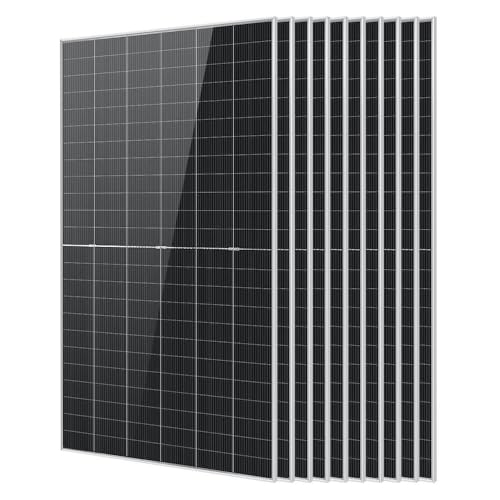
SUNGOLDPOWER UL61730 N-type 10PCS 590W Bifacial Solar Panels,16BB High Efficiency Monocrystalline Solar panel for Energy Storage,Charging Station, Household,On/Off Grid Solar System (10x590W Bifacial)
- High Energy Efficiency: Up to 22.8% energy generation
- Bifacial Technology: Captures up to 30% additional energy
- Durable Construction: Resistant to heat, cold, snow, wind
As an affiliate, we earn on qualifying purchases.
As an affiliate, we earn on qualifying purchases.
Advances in Laser Processing for Photovoltaics
Heterojunction (HJT) solar cells have been among the most efficient types of silicon-based photovoltaics, with record efficiencies exceeding 28%. However, manufacturing challenges—particularly laser patterning-induced damage—have hindered large-scale adoption. Recent research from Longi and Yangzhou University focused on understanding and mitigating shock wave effects during laser processing, a critical step in fabricating rear-side contact structures. Prior efforts have improved passivation and texture, but the new approach directly addresses damage caused by shock waves, which can compromise cell performance and stability.
“Our work not only addresses a major contradiction in laser-based manufacturing but also offers an industry-ready route toward ultra-high-efficiency photovoltaics.”
— an anonymous researcher

Retisee 200pcs 0.5v 400ma Micro Mini Solar Cell for Solar Panels 52mm x 19 Mm/2” x 0.75” Polycrystalline Silicon Photovoltaic Sun Cells Power for DIY Cell Phone Charger
- Lightweight and Portable: Compact and easy to carry
- High Efficiency Polycrystalline Cells: 18% energy conversion rate
- Multiple Connection Options: Series or parallel customization
As an affiliate, we earn on qualifying purchases.
As an affiliate, we earn on qualifying purchases.
Unconfirmed Aspects of Industrial Scalability
It remains unclear how readily this new laser processing technique can be adopted at full industrial scale, including cost implications and compatibility with existing manufacturing lines. Further testing is needed to verify long-term stability and performance under real-world conditions, as well as potential challenges in scaling the textured surface designs.

FellDen Micro Solar Panels with Wire, 5PCS 5V 200mA Photovoltaic Solar Cells Kit
- Package Includes: 5 solar panels with wires
- Panel Dimensions: 110mm x 60mm x 2.5mm
- Application Uses: DIY models, lighting, small appliances
As an affiliate, we earn on qualifying purchases.
As an affiliate, we earn on qualifying purchases.
Next Steps Toward Commercial Application
Researchers plan to collaborate with industry partners to scale up the manufacturing process, evaluate long-term device stability, and explore integration into commercial production. Additional testing and certification will be required before this technology can be adopted in mass-produced photovoltaic modules.

Crown CR-390 6V 390Ah Deep Cycle Battery – BCI 903 L16 – Flooded Lead Acid (Pack of 2)
- Voltage: 6V
- Battery Type: Flooded Deep Cycle
- Capacity (20Hr): 390Ah per battery
As an affiliate, we earn on qualifying purchases.
As an affiliate, we earn on qualifying purchases.
Key Questions
How does the new laser processing method improve solar cell efficiency?
The method reduces shock wave damage during laser patterning, preserving passivation layers and structural integrity, which enhances overall efficiency and stability.
Is this technology ready for commercial production?
While promising, further scale-up, testing, and certification are necessary before it can be widely adopted in industry.
How close is this efficiency to the current world record for heterojunction cells?
The achieved efficiency of 27.27% is very close to Longi’s previous record of 28.13%, indicating it is among the highest reported for this cell type.
What are the main challenges remaining for this technology?
Key challenges include scaling the laser process cost-effectively, ensuring long-term device stability, and integrating the textured designs into existing manufacturing lines.
Source: PV Magazine